
Aluvia Photonics
Founded in 2022 as a spinoff from the University of Twente, Aluvia Photonics pioneers PICs based on aluminum oxide (Al2O3)—a material poised to fill one of the last major gaps within the photonics spectrum.
Unlike indium phosphide, silicon, or silicon nitride (Si3N4) platforms, Al2O3 offers an exceptionally wide transparency window that extends from the deep ultraviolet (~200 nm) to the mid-infrared. It’s uniquely suitable for ultraviolet (UV) photonics, which is an area where existing materials fall short. Aluvia Photonics has demonstrated propagation losses as low as 1–5 dB/m within the telecom band and ~1 dB/cm at 405 nm—setting new benchmarks for low-loss UV operation.
Beyond transparency, Al2O3 can be doped with rare-earth ions to enable active functionality. Erbium-doped devices have achieved ~25-dB fiber-to-fiber net gain, 50-mW output power, and 6-dB noise figures—metrics on par with erbium-doped fiber amplifiers but at a fraction of the size and cost. Thulium-doped devices have produced watt-level continuous-wave outputs and high-peak-power pulse amplification. The platform also has high linearity and power handling, which is ideal for data center and telecom systems that demand signal fidelity.
Aluvia Photonics’ CMOS-process-compatible Al2O3 platform merges the compactness of semiconductor amplifiers with the performance of fiber systems. By extending integrated photonics into the UV and offering active, scalable solutions, the company stands ready to redefine the material foundations of next-generation PICs.
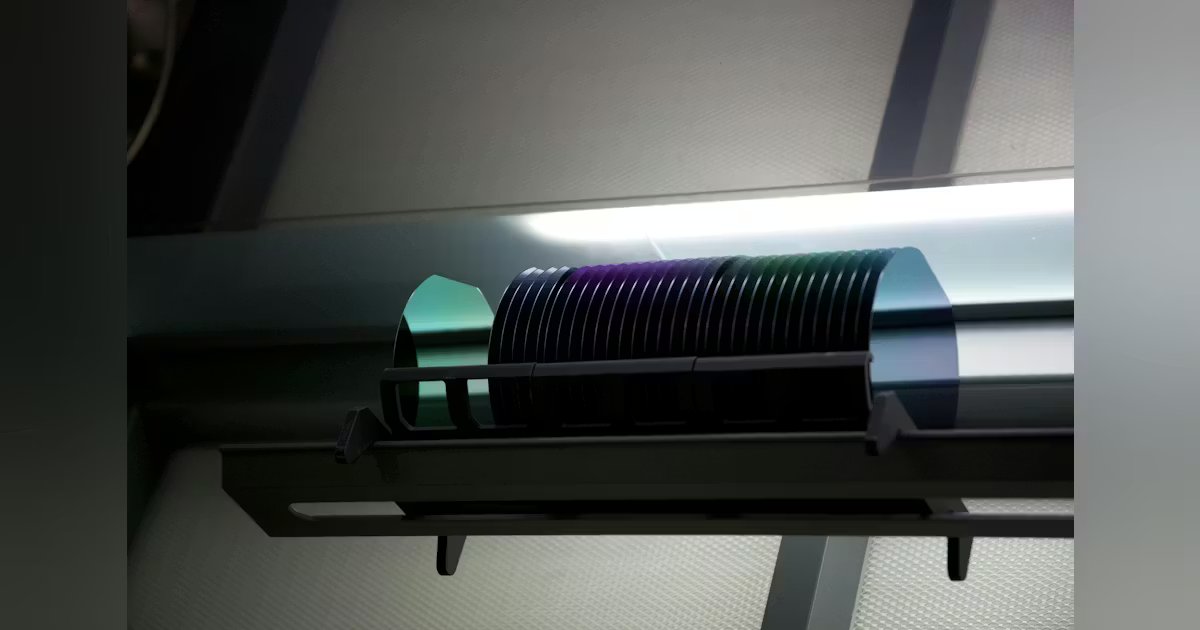
SCIA Systems
Germany-based SCIA Systems makes thin-film process equipment for advanced micro- and nanotechnologies and is applying its expertise in ion beam and plasma technologies to PICs.
For photonics manufacturing, wafer-level performance depends critically on film thickness uniformity and structural precision. SCIA Systems addresses both through two complementary processes: Ion beam trimming and reactive ion beam etching. Ion beam trimming enables sub-nanometer correction of film thickness on 200-mm wafers, which reduces variation from several nanometers to just 0.1-nm root mean square (RMS) roughness.
To refine waveguide geometry, SCIA uses reactive ion beam etching. A focused ion beam cleanly sculpts features with sidewall angles above 75° and sub-nanometer roughness. The process avoids redeposition and damage—even when working with sensitive photoresists or complex multilayer stacks.
SCIA Systems enables the precision control required for high-performance waveguides in materials such as LiNbO3, aluminum nitride (AlN), and Al2O3. Its ion-beam technologies deliver the uniformity, structural fidelity, and yield essential for scaling integrated photonics to industrial production—and it makes SCIA Systems a key enabler within the photonics manufacturing value chain.
Leybold Optics
As PICs advance toward larger wafer formats and tighter performance tolerances, Leybold Optics provides precision surface treatment that bridges optical and semiconductor manufacturing. The company’s ion beam trimming (IBT) and magnetron sputtering technologies enable ultra-uniform, low-loss photonic layers across Si3N4, LiNbO3, and Al2O3 platforms.
Leybold’s 200- and 300-mm systems complement traditional CMP by performing the final planarization step that defines device yield. Ion beam trimming reduces total thickness variation to less than 5 nm and micro-roughness from 0.5 to 0.2 nm to ensure consistent optical properties across the wafer.
Leybold’s magnetron sputtering tools deposit hydrogen-free Si3N4 layers—essential for low-loss waveguides at 1.55 µm and compatible with semiconductor-grade temperature limits. The company collaborates with partners across the photonic ecosystem to qualify these processes for large-scale production.
Along with the materials advances from Aluvia Photonics, CCraft, and SCIA Systems, Leybold Optics completes a critical link in the value chain by delivering the surface precision that turns innovative materials into manufacturable photonic devices.
Recognizing that most material platforms lack native lasing capability, the company developed hybrid laser modules with external gain sections that can be adapted to multiple technologies—including silicon photonics, Si3N4, and Al2O3, the latter in partnership with Aluvia Photonics. These hybrid sources can be tested as standalone evaluation modules or combined with foundry-fabricated circuits, which gives designers a practical route to validate performance before committing to full wafer runs.
By combining multiplatform design expertise with ready-to-integrate laser solutions, the company closes one of the final functional gaps within the PIC ecosystem—and it complements the manufacturing advances of CCraft, SCIA Systems, Aluvia, and Leybold Optics to bring photonic integration closer to industrial maturity.
In conclusion, the field of PICs is undergoing a profound transformation, moving beyond the limitations of silicon. The rise of specialized materials like thin-film lithium niobate, barium titanate, and aluminum oxide is enabling unprecedented performance in speed, energy efficiency, and spectrum of operation. This material revolution, supported by advances in precision manufacturing and cross-platform design, is forging a new, heterogeneous ecosystem. As these technologies mature and scale on larger wafers, they are collectively pushing integrated photonics from specialized research into a new era of industrial-scale production and commercial success.
REFERENCES
1. A. A. Demkov and A. B. Posadas, IEEE J. Sel. Top. Quantum Electron., 30, 8200113 (2024).
2. See www.verifiedmarketreports.com/product/lithium-niobate-ln-modulators-market.