
The semiconductor industry is undergoing one of its most significant transitions since the advent of extreme ultraviolet (EUV) lithography. While transistor scaling continues to drive improvements at the device level, system-level performance is increasingly achieved through advanced packaging technologies.
Architectures based on chiplets, high-bandwidth memory (HBM), and three-dimensional (3D) heterogeneous integration enable higher bandwidth, lower latency, and improved energy efficiency by integrating multiple functions within a single package. The rapid growth of artificial intelligence (AI), high-performance computing (HPC), and data-centric applications is accelerating the adoption of these advanced packaging approaches and places new demands on semiconductor manufacturing.
This evolution is fundamentally changing the requirements of the manufacturing processes. Modern packages combine silicon, glass, low-k dielectrics, metals, polymers, and emerging substrate materials within increasingly compact assemblies. At the same time, wafer thicknesses continue to decrease, interconnect pitches are becoming finer, and acceptable defect levels continue to shrink. Consequently, manufacturing processes such as wafer dicing are no longer regarded as conventional back-end operations but are instead critical drivers of package yield, reliability, and long-term performance.
Ultrafast lasers enable advanced packaging
A range of technologies can meet the increasing demands of advanced semiconductor packaging, and each offers distinct advantages and tradeoffs. As devices continue to shrink and package complexity increases, laser processing is becoming a key enabling technology that offers unmatched flexibility, precision, and reliability for cutting and separating semiconductor devices. From silicon and glass to wide-bandgap materials such as silicon carbide (SiC) and gallium nitride (GaN), laser-based solutions play a critical role across the semiconductor value chain.
Recent advances in laser sources, dynamic beam shaping, high-speed scanning, and AI-assisted process control are further enhancing throughput, yield, and process quality, which makes laser processing a key enabler of next-gen microelectronics and heterogeneous integration.
Lithuanian company EKSPLA developed novel ultrafast laser sources to address the growing demands of the semiconductor and advanced packaging industries. FemtoLux is EKSPLA’s industrial femtosecond laser platform designed for high-precision micromachining within demanding manufacturing environments. By combining ultrashort pulse durations, flexible pulse management, and innovative maintenance-free dry refrigerant cooling, FemtoLux delivers exceptional process stability, high throughput, and 24/7 industrial reliability. Its direct refrigerant cooling (DRC) eliminates water cooling entirely. A hermetically sealed refrigerant loop holds laser temperature within ±0.1°C, which translates into stable long-term output. Active fiber loop (AFL) technology gives the laser burst-mode versatility—megahertz (MHz), gigahertz (GHz), and combined MHz and GHz bursts—so one source can be tuned to the optimal regime for glass, ceramics, polymers, or metals. And as packaging and micromachining applications push for higher throughput, the FemtoLux family scales to meet it—with output up to 50 W of average power and pulse energies as high as 1 mJ.
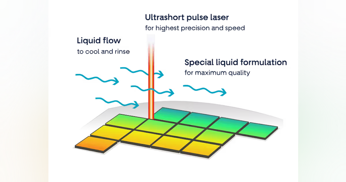
Another interesting example is the LidroCUT process, developed by the German semiconductor equipment manufacturer Lidrotec (see Fig. 1). Their technology combines ultrashort-pulse laser processing with a continuously flowing liquid during ablation. Developed entirely inhouse, Lidrotec is the only company worldwide providing this liquid-assisted laser technology for semiconductor manufacturing. In contrast to conventional dry laser ablation, the liquid simultaneously cools the interaction zone and binds emerging particles. The cooling effect significantly reduces thermal defects such as delamination or melt-burr creation and leads to a very small heat-affected zone (HAZ) within the nanometer range. It also captures ablated material before they can redeposit, which leads to clean, particle-free bonding surfaces.
Water meets lasers: A new era of wafer dicing
Conventional dry laser ablation still presents important challenges when processing advanced packaging materials. Melting, particle redeposition, HAZ, oxidation, and burr formation can compromise edge quality and contaminate bonding surfaces, which leads to additional cleaning or secondary processing steps. Consequently, considerable research is focused on improving laser-material interactions rather than simply increasing processing speed. LidroCUT is designed to overcome these challenges and achieve high-precision, damage-free cutting of semiconductor wafers.
One interesting characteristic of this technology is that the liquid fundamentally changes the laser-material interaction through plume confinement, cavitation bubble dynamics, beam propagation, and hydrodynamic effects, and requires dedicated process development rather than direct transfer of conventional laser ablation parameters. The technology overcomes several limitations of conventional singulation methods by combining high edge quality, low particle contamination, and minimal thermal and mechanical damage, as well as high material independency within a single process step.
The advantages of liquid-assisted ultrashort-pulse laser processing extend well beyond wafer dicing. The same combination of high-precision, low thermal impact, and minimal particle contamination offered by the LidroCUT technology is increasingly important across a wide range of advanced packaging processes. As package architectures continue to evolve, laser processing is expected to play a growing role in the precision structuring of glass substrates and interposers, through-glass via (TGV) fabrication, selective thin-film removal, and other material-specific processing steps. At the same time, next-generation packaging concepts are driving development of integrated thermal management solutions, including microstructured heat spreaders and embedded cooling architectures, which require precise structuring while preserving material integrity. With its ability to process diverse materials while maintaining excellent edge quality and process cleanliness, liquid-assisted ultrashort-pulse laser processing offers a versatile platform for enabling the next generation of advanced semiconductor packaging.
Femtosecond lasers pave way for glass interposers
Glass interposers are poised to redefine advanced semiconductor packaging by providing the scalable, high-density interconnect platform required for the next generation of AI, chiplet, and heterogeneous integration technologies. Glass materials are emerging as a serious alternative to silicon because they are rigid and chemically inert materials and their thermal expansion can be tuned to match surrounding materials. Reaching this potential in production, however, depends on femtosecond laser processes that can structure and metallize glass with the density, precision, and uptime semiconductor manufacturing demands.
EKSPLA’s industrial femtosecond laser platforms meet the requirements of high-quality micromachining of these transparent materials with minimal thermal damage. Glass interposers require thousands to millions of TGVs, and each must meet strict circularity, taper, and crack-free specifications. These requirements can be achieved by the process known as selective laser etching (SLE), a technique that offers exceptional precision and design freedom to enable fabrication of highly complex 3D structures inside transparent materials (see Fig. 2). SLE consists of two complementary steps: An ultrafast laser first induces localized modifications within the bulk of the material (think nanogratings) without affecting the surrounding volume, and a subsequent chemical etching step selectively removes only the laser-modified regions.