
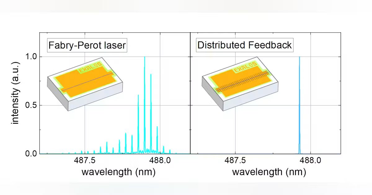
While sub-megahertz linewidths satisfy many quantum operations, some reference sources require even greater coherence. Hybrid architectures that combine DFB lasers with photonic integrated circuits (PICs) are attracting significant interest. Integrated resonators, stabilization structures, and optical feedback elements can further narrow effective linewidth of semiconductor technologies.3 Such approaches may ultimately provide a path toward highly scalable quantum systems built from standardized laser and photonic building blocks.
Unlike external cavity systems, this approach avoids mechanical tuning elements. The absence of mode hops across the usable range simplifies system control and reduces the need for active feedback, which is particularly beneficial for cooling or trapping sequence applications that require dynamic frequency sweeps.
Reliability and operational stability
Reliability is critical for deployable quantum systems. Semiconductor DFB lasers benefit from established manufacturing and reliability models. Lifetime testing indicates stable operation of more than 10,000 hours under constant power, with moderate current increase over time. Eliminating external cavities also improves robustness against vibration and temperature variation. These characteristics enable use in compact field-deployed systems for which environmental control is limited.
Manufacturing scalability
A key advantage of DFB technology is compatibility with wafer-scale semiconductor processing. Using metal-organic chemical vapor deposition (MOCVD)-grown GaN substrates, devices can be produced with high uniformity and throughput. Production volumes of millions of devices per year are feasible, with wavelength control typically within ±1 nm across wafers. It enables standardized components and scalable multichannel architectures.
Implications for quantum systems
Simplified laser subsystems directly impact system scalability. In quantum computing, reduced optical complexity enables expansion toward larger qubit counts. For sensing, compact and robust sources support deployment in real-world environments. For communications, manufacturable components enable practical quantum network infrastructure. The broader trend is clear: As quantum technologies transition from research instruments to engineered products, laser architectures must evolve from precision laboratory assemblies toward scalable semiconductor platforms.
Laser subsystem complexity has been a persistent constraint in quantum system design. ECDL, fiber laser, and frequency-converted architectures deliver high performance but often impose penalties in size, complexity, and operational robustness.
Visible DFB lasers offer an alternative approach by integrating wavelength selection directly within the semiconductor source. Combined with semiconductor amplification and photonic integration, they provide a viable path toward scalable quantum photonics. As quantum technologies transition from demonstrations to commercial systems, the ability to replace complex optical assemblies with compact manufacturable semiconductor devices may prove as important as any advance in the quantum hardware itself.
REFERENCES
1. M. Rossetti, M. Malinverni, A. Castiglia, and M. Duelk, Proc. SPIE, 13912, 1391209 (Mar. 5, 2026); https://doi.org/10.1117/12.3080363.
2. M. Malinverni, M. Rossetti, A. Castiglia, and M. Duelk, Proc. SPIE, 13912, 139120A (Mar. 5, 2026); https://doi.org/10.1117/12.3081262.
3. G. Perin et al., Proc. SPIE, PC14090, PC140900A (May 28, 2026); https://doi.org/10.1117/12.3099267.