
Figure 1c shows a configuration for wafer-level applications scalable to different sizes by selecting appropriate F-theta focal lengths. For example, a 300-mm focal length system provides coverage for 200- to 300-mm wafers with spot sizes of 10 to 50 μm for scribing.
Double-sided scribing. Silicon wafers for power semiconductors and solar cells require scribe lines on both surfaces for controlled cleaving. Simultaneous scribing provides front-to-back alignment while eliminating wafer flipping, improving throughput. Symmetric scribing may also improve cleave quality and reduce edge chipping.
Inspection applications. The dual-sided line configuration enables simultaneous optical inspection of both surfaces for bifacial solar cells and thinned semiconductor wafers, and potentially increases inspection throughput. It also reduces handling and enables correlation of defects between surfaces.
Concept versatility
The optical setup can be modified for custom specifications such as:
Multi-beam configurations. The double-spot splitter can be replaced with multibeam elements (3, 4+ beams) for processing from multiple angles or creating redundancy.
Dynamic scanning. Static mirrors can be replaced by galvo scanners for extended area coverage and pattern generation.
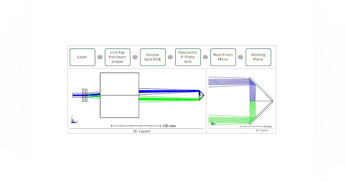
Flexible beam shaping. The line shaper can be replaced by circular top hat, rectangular, or custom profiles depending on application requirements. For applications requiring tight focusing (such as wafer scribing), the beam shaper can be omitted entirely to achieve diffraction-limited spot sizes.
Adjustable working envelope. System accommodates different substrate thicknesses (0.5 to 10+ mm typical) by repositioning mirrors.
Scalable architecture. System is scalable to different working envelopes by selecting appropriate F-theta focal lengths (100 to 300 mm typical) while maintaining high-quality focusing performance.
Wavelength flexibility. Concept is wavelength-agnostic and applicable to ultraviolet (UV), visible, infrared (IR), and ultrashort-pulse lasers.
Inspection integration. For inspection applications, cameras or detectors can be integrated to capture images or signals from both sides simultaneously, with the laser providing line illumination.
We believe this approach combined with Holo/Or’s diffractive optical elements shows potential to enable efficient and economical manufacturing solutions. Its modular design allows extensive customization for specific applications, wavelengths, and power levels. Further experimental work is needed to validate these concepts and explore their practical implementation.
REFERENCES
1. A. Völl, J. Stollenwerk, and P. Loosen, Laser Tech. J., 15, 1, 42–45 (2018).
2. J. Meinschien, C. Stauch, T. Schubert, and S. Hellstern, PhotonicsViews, 19, 5, 48–51 (2022); https://doi.org/10.1002/phvs.202200037.
3. S. Gräf and F. A. Müller, Sci. Rep., 11, 22944 (2021); https://doi.org/10.1038/s41598-021-02290-3.