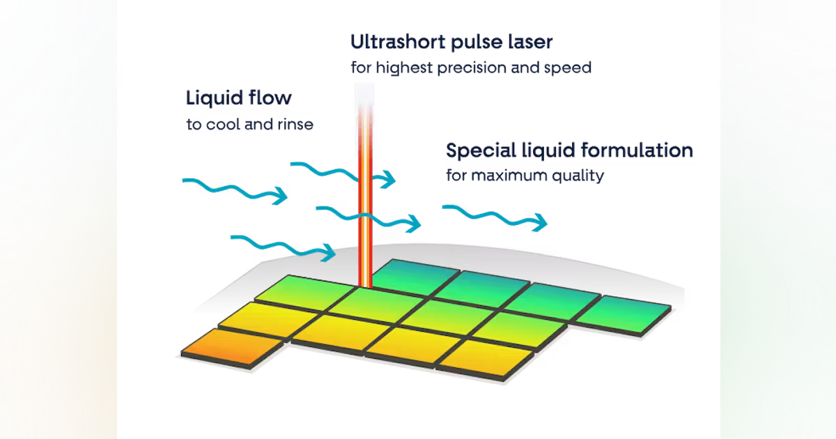
Laser processing: Powering next-gen semiconductors
The semiconductor industry is undergoing one of its most significant transitions since the advent of extreme ultraviolet (EUV) lithography. While transistor scaling continues to drive improvements at the device level, system-level performance is increasingly achieved through advanced packaging technologies. Architectures based on chiplets, high-bandwidth memory (HBM), and three-dimensional (3D) heterogeneous integration enable higher bandwidth, lower
Laser processing: Powering next-gen semiconductors Read More »