
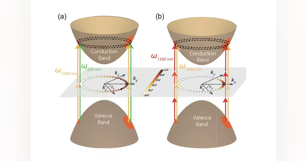
Electrical current shows sensitive response to relative optical phase
One of the coolest aspects of this work for Gong was discovering just how sensitively the electrical current responds to the relative optical phase. Because the current is controlled by the relative phase between the two absorption pathways, a change in optical path length of only tens of nanometers can produce a visible change in the measured signal.
“We could tap the optical table and immediately see the current respond,” Gong says. “Even small air fluctuations along the beam paths could shift the relative phase enough to alter the signal. It was remarkable that such tiny and otherwise invisible optical disturbances could be converted directly into a measurable electrical response.”
The same current was also extremely sensitive to the direction of the optical polarization. Rotating the polarization didn’t merely change the current’s amplitude—it changed the direction in which the carriers were injected. “When we rotated the polarization by 90 degrees, the signal disappeared from one pair of electrodes and emerged in the perpendicular pair,” says Gong. “Our major ‘aha!’ moment grew directly out of this sensitivity. When we initially scanned the two pulse trains through one another in time, we could see a broad, noisy envelope around their temporal overlap, but the coherent structure within it was obscured. The signal indicated that the two quantum pathways were interfering, but the relative phase was too noisy for the underlying interference to appear clearly.”
This instability came from the offset-frequency noise of the frequency comb. Because the comb’s offset frequency also provided the reference for the group’s lock-in detection, its broad linewidth—initially on the order of hundreds of kilohertz—made it difficult for the lock-in amplifier to extract the signal with a satisfactory signal-to-noise ratio.
“We used a feed-forward loop with acousto-optic modulators (AOM) to compensate for the offset-frequency noise and narrowed its effective linewidth from hundreds of kilohertz to approximately 1 Hz,” says Gong.
After the offset frequency was stabilized, the measurement changed dramatically: Clear sinusoidal fringes appeared inside what had previously looked like a noisy envelope. The fringes were produced by the controlled modulation of the relative optical phase—a direct electrical signature of quantum interference. “It felt almost as if the quantum interference had crystallized out of the noise,” says Gong. “What had appeared disordered suddenly became structured, reproducible, and controllable.”
Another unforgettable moment was “when we rotated the polarization while measuring both orthogonal current components simultaneously,” says Gong. “As the polarization rotated by 90 degrees, the current disappeared from one electrode pair and appeared in the other. At one orientation, one component reached its maximum while the perpendicular component approached zero. After the rotation, their roles were reversed. Seeing this transfer occur between the two channels made the vector nature of the current immediately visible.”
Challenge: Device fabrication
Beyond suppressing the different sources of optical and frequency-comb noise, one of the group’s biggest technical challenges was fabricating the device itself. It required two orthogonal pairs of micron-scale electrodes to form reliable ohmic contacts with the AlGaAs sample.
The “established 1 + 2 QuIC device architectures available to us were based largely on Schottky-contact geometries,” Gong explains. “For our 2 + 3 QuIC measurement, we needed ohmic contacts to minimize contributions from built-in electric fields and directly isolate the optically injected ballistic current. There was no established recipe we could simply follow for our particular AlGaAs structure and device geometry, so we had to develop much of the fabrication process through systematic experimentation.”
Forming an ohmic contact depends sensitively on the semiconductor-metal interface, the composition and sequence of the deposited metal layers, their individual thicknesses, and the annealing temperature and duration. “We explored different metal stacks and annealing conditions, and used a plasma etch to remove the native oxide from the AlGaAs surface before depositing the contacts,” says Gong. “Even small changes in these steps can determine whether the final device behaves as a low-resistance ohmic contact or retains a nonlinear, Schottky-like response.”
The staff and instrumentation at the University of Michigan’s Lurie Nanofabrication Facility “was essential to this exploration,” Gong adds. “Solving the contact problem ultimately allowed the device to provide a direct electrical readout of the directional ballistic current.”
Theoretical work
The group’s experiment was motivated by the remarkable theoretical prediction from Professor John Sipe and his collaborators, and Gong extended it to what they could directly measure experimentally by developing an optoelectronic response model that connects the microscopic angular distribution of the injected carriers in k-space to the macroscopic current collected by their two orthogonal electrode pairs in real space.
“Our model incorporates the nonlinear optical response of AlGaAs, the polarizations of both optical fields, and the finite geometry of the electrodes,” says Gong.
The same model closely reproduced the detailed polarization dependence observed during their experiment while remaining consistent with the original prediction of a more localized carrier distribution in k-space. “I find it especially satisfying that it brings two levels of the physics into a single framework,” says Gong. “Fundamental quantum-interference phenomenon of momentum-space localization and its experimentally accessible manifestation as a directional, vector-resolved electrical current. In other words, the model shows how an invisible microscopic carrier distribution becomes a current that we can measure directly at the contacts.”
Optical metrology, electronic and quantum materials studies ahead
Gong sees two complementary application directions for this work: Precision optical metrology and the study of electronic and quantum materials.
“The first is for phase-sensitive detection of optical frequency combs,” Gong says. “Conventional electronics can’t directly follow an optical field oscillating at hundreds of terahertz. Quantum interference provides a way to translate this otherwise inaccessible optical phase information into a much lower-frequency electrical signal.”
For the group’s experiment, the current depends sensitively on the relative phase between two multiphoton absorption pathways. For a frequency comb, this relative optical phase evolves with the carrier-envelope offset frequency so the semiconductor effectively acts as a phase-sensitive optical-to-electrical mixer: Information carried at optical frequencies appears as a measurable current oscillation in the radio-frequency range.
“This could provide an extremely sensitive tool for detecting and stabilizing the offset frequency, relative phase, timing, and phase noise of frequency combs,” Gong points out. “The directional 2 + 3 current adds a vector-resolved and polarization-sensitive electrical response to this phase detection.”
A second direction is momentum-selective spectroscopy of electronic materials. By optically injecting carriers into a narrow range of directions and measuring the resulting vector current, researchers can explore how band anisotropy and local electronic structure govern carrier motion and scattering. “Extending the method beyond AlGaAs to transition-metal dichalcogenides, multivalley systems, and spin-textured or topological materials could provide a new route toward studying valley and spin dynamics—and, with appropriate theoretical modeling, potentially aspects of Bloch-band quantum geometry such as Berry curvature,” says Gong.
“As a research tool, our technique is ready now for ultrafast and frequency-comb laboratories,” says Gong. “Our near-term goal is to improve its sensitivity and stability and explore its use as a vector-resolved detector of optical phase and polarization.”
The next scientific step? Extend the method “to other materials and use wavelength, phase, and polarization to address different regions of momentum space,” Gong adds. “We’re particularly interested in anisotropic, multivalley, spin-textured, and topological materials, in which the directional current may reveal new information about band structure, carrier scattering, valley and spin dynamics, and potentially quantum geometry. Translating the concept into a compact practical device is a longer-term goal.”
FURTHER READING
Y. Gong, K. Wang, and S. T. Cundiff, Phys. Rev. Lett., 137, 036901 (Jul. 16, 2026); https://doi.org/10.1103/3v91-5pzf.